
NEWS
Modi Opens Semicon 2026 With a Two-Stage Chip Bet
At Semicon India 2026, Modi is selling a second subsidy round while three packaging plants ship and the first commercial fab remains due in 2028.

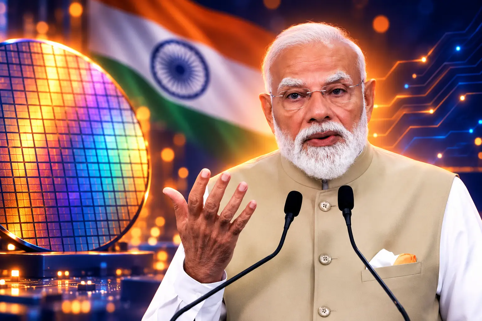
Prime Minister Narendra Modi opened SEMICON India 2026 in New Delhi on September 17, courting chip investors as three Indian plants already ship packaged devices. The first commercial silicon fab is still scheduled for 2028. The three-day meeting at Yashobhoomi runs through September 19.
He is not selling a finished foundry industry. He is selling a second, wider subsidy round, a cluster of assembly lines that have begun to move product, and a promise that toolmakers and chemical firms will put down roots before the Dholera wafers start.
Two Subsidy Rounds Now Exceed ₹2 Lakh Crore
The India Semiconductor Mission, run by the Ministry of Electronics and Information Technology, first got Cabinet backing on December 15, 2021, with Semicon 1.0 at ₹76,000 crore. The Union Cabinet cleared Semicon 2.0 on July 15, 2026, with a ₹1,27,500 crore Semicon 2.0 outlay (about $13.3 billion), and the scheme was notified on August 31, 2026. Together the two official fiscal rounds come to ₹2,03,500 crore.
That is the wager on the table. It is not a cheque that has already been spent on working fabs. It is policy cover for plants that pass technical and financial tests, paid as projects go up.
THE TWO SEMICON LEDGERS
| Programme | Fiscal outlay | Cleared | What it pays toward |
|---|---|---|---|
| Semicon 1.0 | ₹76,000 crore | December 15, 2021 | Silicon and display fabs, compound plants, packaging, design incentives |
| Semicon 2.0 | ₹1,27,500 crore | July 15, 2026 | Design, machines and materials, more fabs, packaging, research, talent |
A Cabinet note on the second round said twelve manufacturing units had been approved under the first phase, with committed investment of more than ₹1.64 lakh crore. The mix is the tell. The government listed one silicon fab, one silicon-carbide fab, one integrated gallium-nitride Micro-LED display fab, and nine packaging units.
Electronics and IT Minister Ashwini Vaishnaw said Semicon 2.0 is built on six pillars: chip design, machines and materials, more fabs, stronger assembly and test, research, and talent. The machines-and-materials line is new money for an industry that still has to import the tools and wet chemicals a fab cannot run without.
Pranay Kotasthane, deputy director at the Takshashila Institution, put the political point in plain language before the hall opened. Semicon in New Delhi, he said, is Modi’s way of signalling a long-term commitment to growing the chip industry, and that is the message to global investors.
The first electronics subsidy round, in 2020-21, helped Apple expand iPhone making in India, and the company now builds about 25 percent of that device in the country. Chipmaking is a slower clone of that playbook. Phones can be assembled in a few years. A commercial wafer fab is a decade-class object even when the money is waiting.
Three Plants Are Already Shipping Packaged Chips
The live industry is still the back end of the chain: take a finished wafer made elsewhere, saw it, package it, test it, and ship a labelled part. Micron Technology, Kaynes Semicon, and CG Semi are the three names the Cabinet note put in commercial production, with one more unit expected to start in 2026.
THE PLANTS THAT MATTER RIGHT NOW
| Project | Place | What it does | Status |
|---|---|---|---|
| Tata Electronics with PSMC | Dholera, Gujarat | CMOS silicon fab, 28-110 nm, 50,000 wafers a month | Under construction, due 2028 |
| Micron Technology | Sanand, Gujarat | DRAM and NAND assembly and test | Commercial production since February 28, 2026 |
| CG Semi (CG Power, Renesas, Stars Microelectronics) | Sanand, Gujarat | Outsourced assembly and test | Commercial production, July 2026 |
| Kaynes Semicon | Sanand, Gujarat | Outsourced assembly and test | Commercial production, March 2026 |
| Tata Semiconductor Assembly and Test | Jagiroad, Assam | Assembly, test, marking and packaging | Under construction |
Sanjay Mehrotra, Micron’s chief executive, told the New Delhi hall on September 17 that Sanand will move from tens of millions of chips in 2026 to hundreds of millions in 2027. Finished DRAM and NAND products are leaving the site with a Made in India label, he said, and current output already exceeds the memory India’s laptop market needs. The first shipment of India-made memory modules went to Dell for laptops built and sold in the country.
For decades, people have talked about India’s semiconductor potential. I have been in many of those conversations. Potential does not ship products. What I see in India today is execution.
Sanjay Mehrotra, chief executive, Micron Technology, at SEMICON India 2026
Sanand is still an assembly and testing hall. It receives advanced DRAM and NAND wafers from Micron’s global network and turns them into finished memory and storage. The Indian approval ledger puts the project at ₹22,516 crore. Mehrotra said Micron has been in India for seven years, directly employs more than 7,000 people, and that India teams have contributed to more than 3,700 patents, inventions and disclosures.
CG Semi, a joint venture of CG Power with Renesas of Japan and Stars Microelectronics of Thailand, was opened by Modi on July 4, 2026, in Sanand. Kaynes was opened on March 31, 2026. Tata’s Assam plant, listed at ₹27,120 crore, is still being built. HCL’s display-driver unit with Foxconn near Jewar in Uttar Pradesh is also under construction, along with smaller compound and packaging jobs in Odisha, Punjab, Andhra Pradesh and Surat.
Dholera’s First Commercial Fab Is Due in 2028
The plant that would make India a wafer country rather than a packaging country is Tata Electronics’ CMOS fab at Dholera, partnered with Powerchip Semiconductor Manufacturing Corporation of Taiwan. The April 2026 official project cost is ₹91,526 crore. Planned output is 50,000 twelve-inch wafers a month at 28 nanometre to 110 nanometre nodes, the workhorse processes used in cars, industrial controllers, power-management chips and display drivers.
Those nodes are not the leading-edge silicon that trains large AI models. Taiwan still accounts for more than 60 percent of global foundry revenue and more than 90 percent of leading-edge chips, according to a April 2026 paper from the Center for Strategic and International Studies. East Asia holds more than 75 percent of manufacturing capacity. India’s first commercial fab is being aimed at the durable middle of the market, where demand is steady and the process recipes are older.
Even that middle is slow. Tooling has to be installed, process recipes transferred from PSMC, and yields beaten into shape wafer by wafer. The government schedule for commissioning remains 2028. Until those lines are up, every “Made in India” memory module leaving Sanand still begins as a wafer made in another country.
Design is the other Indian strength, and it does not need Dholera to exist. Nearly all of the top 25 design firms already keep large engineering offices in Bengaluru, Hyderabad and Noida. Semicon 2.0 tries to pull some of that work into Indian-owned IP and into the new plants, with 24 design projects already approved for financial support and 105 startups and MSMEs given access to industry-standard design software.
Toolmakers and Chemists Filled the Front Row
The guest list on September 16, the night before the hall opened, showed who has to say yes before a fab is real. Modi chaired a roundtable at Seva Teerth with SEMI, the global industry body co-organising the 2026 edition, and with the firms that sell scanners, etchers, testers, gases and wet chemicals.
WHO SAT IN THE ROUNDTABLE
- Lithography and tools: ASML, Applied Materials, Tokyo Electron, Lam Research and Advantest, the vendors that sell the machines a fab cannot substitute.
- Materials: Merck and Fujifilm, which mix the process chemicals and surface treatments used on wafers.
- Chip companies: Micron, Infineon, AMD, Intel, NXP and Rapidus, plus IBM Research.
- Plants on the ground: Tata Electronics, CG Power and Foxconn, the groups already building or assembling in India.
A foundry announcement makes a better headline. A materials plant is what a foundry drinks. Fujifilm had already signed a Gujarat pact to study a materials production base in Dholera. On September 16, after its chief executive sat in the roundtable, the company said it would invest about ₹800 crore ($83 million) in a greenfield semiconductor-materials facility in India, in two phases starting October 2026, with commercial production expected in fiscal 2028. Phase one is front-end process chemicals. Phase two, timed to how fast the local industry actually grows, is surface-conditioning materials and high-purity chemicals. Fujifilm said it wants support under Semicon 2.0.
Fiscal 2028 is the same window as Tata’s Dholera fab. That is not a coincidence. You do not run 50,000 wafers a month on air-freighted bottles if you can avoid it. The second subsidy round’s machines-and-materials pillar exists because the first round bought packaging halls and one unfinished fab, not a local supply chain.
Country pavilions at Yashobhoomi belong to Japan, South Korea, Malaysia, the Netherlands, Singapore and Sweden, a map of tool, chemical and packaging power rather than a map of AI-chip glamour. Twelve Indian states have booths. The official theme is “Silicon to Systems: Building the Ecosystem,” and the floor includes a startup pavilion, a student hackathon and a workforce stand beside the vendors.
Water, Talent and the Hard Part of a Fab
Worldwide chip sales hit $791.1 billion in 2025, and forecasts cited in the CSIS paper put the 2026 market close to $1 trillion. India’s own chip market is projected at more than $100 billion in revenue by 2030 by the India Electronics and Semiconductor Association and Counterpoint Research. The gap between those numbers and three packaging plants is the labour and utilities problem, not the conference agenda.
INDIA’S CHIP TALENT MATH
- Design bench: India has about 120,000 chip-design engineers, about 20 percent of global chip-design talent, which is why the big design houses are already here.
- Skill filter: Roughly 600,000 engineers graduate in electronics-related fields each year, but less than 1.5 percent have the skills needed to join a semiconductor workforce.
- Projected gap: One tally cited by CSIS put a shortfall of 300,000 semiconductor workers by 2027, covering process, equipment, yield and fab operations, not only design.
- Training pipeline: The Chips to Startup programme targets 85,000 industry-ready design professionals, with about 68,000 students trained by August 2026, while Lam Research has committed to train 60,000 engineers over 10 years on its Semiverse platform.
Design talent is the easy Indian story, because it already exists in three metro cities. Process engineers, equipment technicians and yield managers are the scarce ones, and they have to live next to Sanand, Dholera, Jagiroad and Jewar, not next to a Bengaluru design centre. Modi used the roundtable to push skilling, including a government target of training one crore people in AI, and to ask the visiting firms to put their own training money beside the state’s.
Fabs also need ultra-pure water and power that does not blink. A missed second during a process step can scrap a wafer lot. Water-system firms working with Indian sites say the constraint is a mix of availability and reliability, because source quality changes by region and a fab cannot let that variability into the line. Gujarat is stacking extra state support on top of the central grant, including cheaper power, but the physics of a cleanroom does not care about a press note.
Modi Says the World Needs New Chip Hubs
The fifth edition of SEMICON India is jointly organised by the India Semiconductor Mission, the electronics ministry and SEMI. A Prime Minister’s Office note the day before the opening listed more than 600 companies taking part, representatives from 52 countries, around 50,000 expected visitors, more than 400 executives and over 150 speakers, across about 15,000 square metres. About 300 of the companies are international.
Modi told the CEOs on September 16 that the government would keep “a predictable and responsive policy environment,” and that India should aspire to be among the early leaders in emerging technologies, including AI and quantum computing. On September 17, after walking the exhibition floor, he made the strategic pitch the subsidies are built to serve.
The semiconductor industry is facing numerous challenges. Amidst these challenges, the world is in dire need of new and reliable manufacturing hubs. I assure you that India is continuously preparing itself for this role.
Narendra Modi, Prime Minister, addressing SEMICON India 2026
India's semiconductor ecosystem is expanding rapidly. It is opening new opportunities for innovation, investment and growth. Addressing SEMICON India 2026 in Delhi. https://t.co/a7A2Rs89DI
— Narendra Modi (@narendramodi) September 17, 2026
Mehrotra tied Micron’s Gujarat ramp to the same AI wave, arguing that models do not run without memory and storage. That is a fair claim for a packaging plant that finishes DRAM and NAND. It is not the same claim as making the accelerator silicon those models sit on. India’s bet, as written in the two ledgers, is to own more of the chain around that silicon: design, packaging, materials, and one commercial CMOS fab at mature nodes by 2028.
The three-day meeting ends on September 19. Fujifilm’s chemicals plant is due in fiscal 2028, the same window as Tata’s Dholera fab, which is when the wager stops being a conference and starts being a yield number.

A CubeSat Will Age Whisky That Never Comes Home

A Charity Quote Cost Shia LaBeouf the FKA twigs NDA

Looker Turned a Model’s Body Into Ad Inventory

Infinity Ward Bets a Paid DMZ Will Stick This Time

Disney Sidesteps a Kimmel Renewal as Failla Cites Losses

How to Get Pre Boarding on Southwest – Skip the Line with These Tricks

False AI Intel Nearly Put US Crews on a Chinese Ship

Tim Cook’s $4.6 Trillion Apple Still Runs on One Phone

OpenAI Posts a Navier-Stokes Proof Clay Has Not Touched

Dunes Air Sues Nora Fatehi Over Its Luxury Jet
-
 TRAVEL3 years ago
How to Get Pre Boarding on Southwest – Skip the Line with These Tricks
-
 NEWS1 month ago
False AI Intel Nearly Put US Crews on a Chinese Ship
-
 BUSINESS2 months ago
Tim Cook’s $4.6 Trillion Apple Still Runs on One Phone
-
 NEWS2 months ago
OpenAI Posts a Navier-Stokes Proof Clay Has Not Touched
-
 ENTERTAINMENT2 months ago
Dunes Air Sues Nora Fatehi Over Its Luxury Jet
-

 LIFESTYLE3 years ago
How Often Do You Have to Change a Monkey’s Diaper? The Truth About Pet Monkeys
-

 NEWS2 months ago
Australia Treats Cloud Software Payments as Taxable Royalties
-

 LIFESTYLE3 years ago
How Long Does It Take for Armpit Hair to Grow? The Stages of Hair Growth and How to Shave It